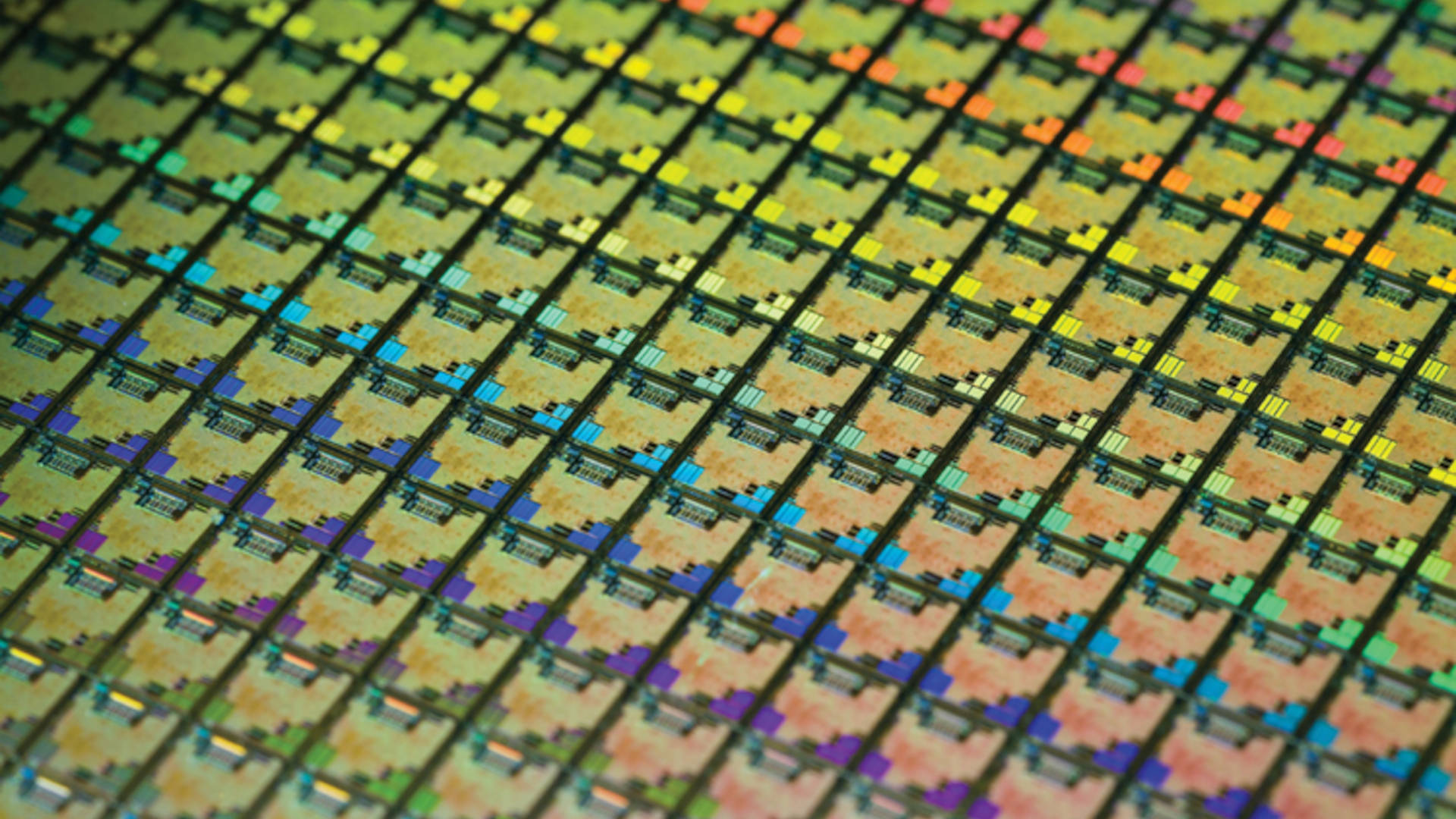
Found this in a dumpster near TSMC fab, how to cut this into usable GPU? from r/pcmasterrace
‘Chip binning’ is supposed to be the process of testing newly manufactured silicon to see how many of the important bits work and how high the thing will clock. But TSMC seems to be taking the notion a little too literally, as one Redditor found when they apparently discovered an entire TSMC wafer in dumpster.
The aptly monikered Redditor, AVX512-VNNI, says the wafer, which appears to be fully intact, was found discarded at TSMC’s Fab 16 chip factory or fab in Nanjing, China. While it’s not the most advanced fab in the world, it is still producing 12nm silicon, which is fairly high tech.
On Reddit, AVX512-VNNI pondered how the wafer, which visibly contains scores of chip dies, might be cut up into usable GPUs. But it wasn’t a serious query.
As AVX512-VNNI points out, the wafer doesn’t contain any customer chip designs. Instead it’s a test wafer containing dummy circuitry layouts used to evaluate the performance and calibration of the hyper-complex lithography machines that etch the patterns onto the wafer that are then cut up into chips.
Still, it’s a good opportunity to speculate over the best way a keen enthusiast might try to cut the wafer into individual chips. Diamond tipped pizza slicers are the obvious choice. That said, the mere 0.5mm gaps between the chips would call for a very steady hand.
Actually, you’d need a bit more than that. Over to another Redditor for a précis of what’s really required.
“You just need to have a clean room. And by that I mean a room with absolute zero dust. Then you will need a special wire cutter. Not wirecutter – a wire cutter, that is a machine with a thin wire that cuts wafer into chips and minimizes dust. After that, you need an assembly machine that will place your chips onto a substrate with submicron precision. And, of course, you’d need a working PCBs with all components. Easy-peasy.“
And, you might say, lemon squeezy. Of course, an easier solution might just be to wire up the whole wafer as a single chip and side step the whole slicing malarkey. That’s actually a thing and it’s called ‘wafer-scale’ computing. You’d need a lot of thermal paste, of course, and the power requirements would put even melting Nvidia RTX GPUs to shame.
Overall, Redditor AVX512-VNNI does seem to be suspiciously well informed on the subject of chip production, which does rather beg the question of exactly how serendipitous the discovery of the wafer really was… But it’s a fun discovery all the same.
